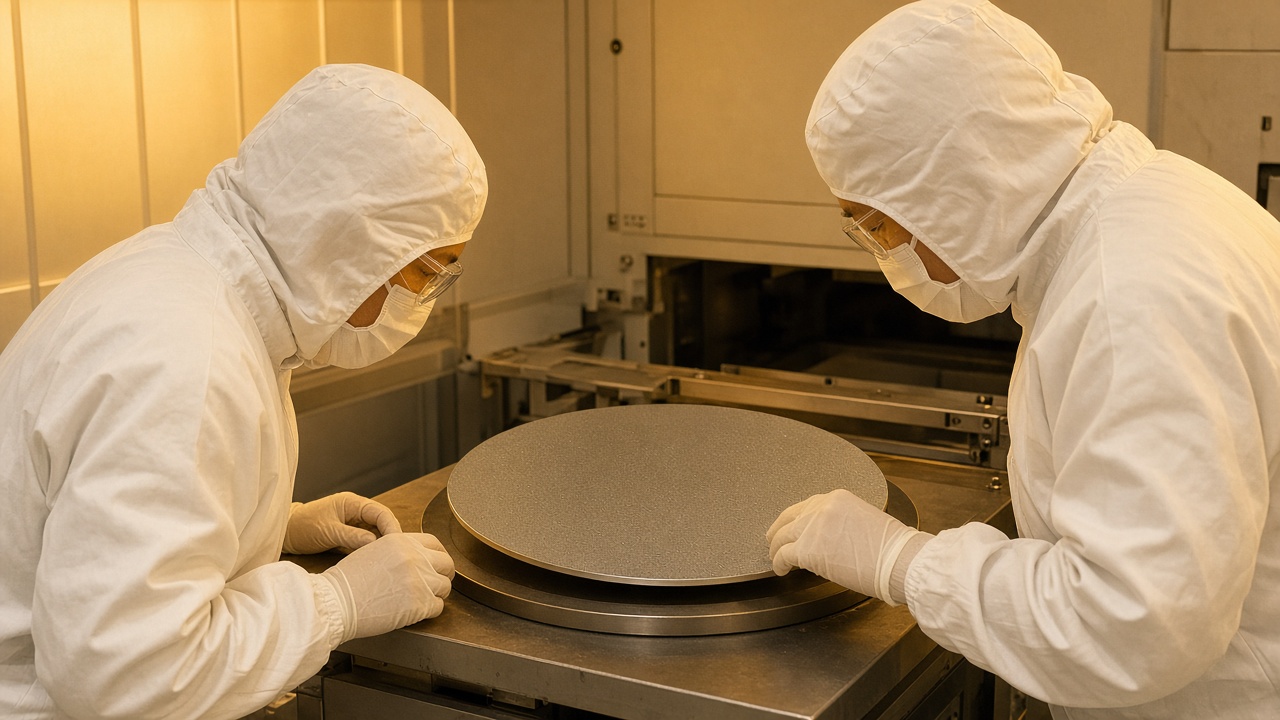
Resonac Holdings said it has developed Japan’s first 300-millimeter silicon carbide substrate, a materials breakthrough that could let power-semiconductor fabs print roughly four times as many devices from each wafer compared with today’s smaller formats.
The Tokyo-based supplier, formed from the 2023 integration of Showa Denko and Resonac’s predecessor businesses, announced the milestone on Monday as chip makers worldwide hunt for ways to cut cost per device in electric vehicles, data-center power electronics, and industrial drives. Silicon carbide handles high voltage and heat better than conventional silicon, but wafers have been expensive partly because substrates are difficult to grow at scale without defects.
Why wafer size matters
Moving from 150-millimeter or 200-millimeter silicon carbide to a 300-millimeter platform mirrors the decades-long shift in mainstream silicon, where larger diameters spread fixed processing costs across more dies. Nikkei Asia reported that Resonac is the first Japanese company to produce a 300-millimeter SiC substrate, placing it alongside U.S. and Chinese competitors that have been racing to prove the larger boules can survive slicing, polishing, and epitaxy without cracking.
Commercialization timelines were not finalized in the company’s initial disclosure, and industry analysts caution that demonstration wafers often spend years in qualification before a automaker or cloud provider will sign a volume contract. Still, the announcement gives Japan’s Ministry of Economy, Trade and Industry another domestic success story as it subsidizes materials and equipment makers to reduce reliance on foreign substrate supply.
Supply chain and customer tests
Power-device manufacturers typically require months of reliability testing on sample wafers before redesigning fabs. Resonac will need to show uniform crystal quality across the wider surface, a challenge that has kept some rivals on smaller diameters even after laboratory successes. Partnerships with integrated device manufacturers and foundries will determine whether the 300-millimeter line becomes a catalog product or a bespoke offering for a handful of strategic accounts.
For Japan’s semiconductor policy, the timing aligns with renewed investment in Kumamoto and other hubs hosting logic and memory plants: if substrate scale-up succeeds, downstream fabs in the region could source advanced power materials closer to home rather than importing finished wafers.
Competition and next steps
Global leaders in silicon carbide have already publicized road maps for 200-millimeter and 300-millimeter production, meaning Resonac’s claim is as much about joining an elite tier as about inventing the category. Investors will watch capital expenditure guidance, yield data, and whether the company secures co-development deals with automakers pushing 800-volt architectures.
Until customer qualifications conclude, the development remains a materials-science headline with industrial consequences still pending. If yields hold, however, Japan gains a domestic option in one of the most bottlenecked layers of the EV and AI power stack.