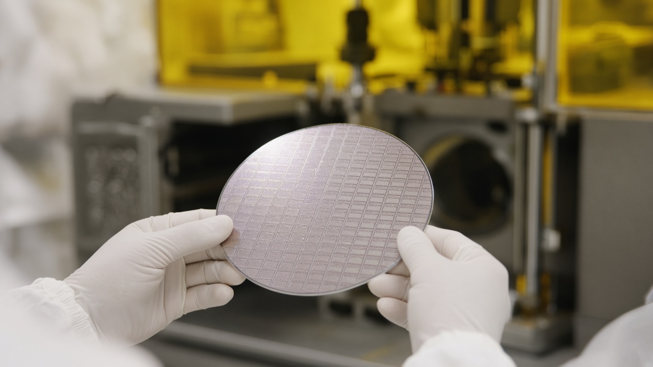
Researchers led by KAIST professor Kang Ki-bum steered where two-dimensional molybdenum disulfide crystals begin to grow, centering nucleation in more than 99 percent of 400 experimental patterns and offering a path toward vertically stacked AI processors with lower power draw.
The Ministry of Science and ICT highlighted the work on October 8 after its publication in Nature. Collaborators at Ulsan National Institute of Science and Technology, Hanyang University, and TDS Innovation helped pattern oxide barriers that release oxygen to suppress crystal seeds near edges while allowing a single nucleus in the middle of each site.
Mechanism
Molybdenum disulfide is a candidate channel material for ultra-thin transistors, but random nucleation has made uniform films difficult. By exploiting stronger oxygen suppression at barrier edges, the team drew growth toward the center, producing single crystals across hundreds of lithographed windows.
Kang said the result confirms that nucleation location can be engineered, not merely hoped for, in 2D semiconductor growth. The group plans to integrate the technique with existing wafer tools rather than bespoke lab-only processes.
Industry relevance
Stacked memory and logic—critical for on-device AI—need precise layer alignment. If nucleation can be pinned, downstream etch and transfer steps become more predictable, potentially reducing yield loss that has kept 2D materials in research fabs.
MSIT research policy chief Kim Sung-soo framed the paper as basic science converted into manufacturable know-how, a priority as Seoul funds both DRAM giants and startup foundry services.
What remains
The study proves location control on patterned coupons, not yet on full 300-millimeter production lines. Scaling will require matching oxygen release kinetics with high-volume deposition tools. Even so, equipment vendors in Yongin and Pangyo said they are tracking the process for possible pilot lines aimed at low-power edge accelerators.
Funding path
The project drew support from the Ministry of Science and ICT's next-generation semiconductor programs, which are separate from the larger DRAM capex packages led by private chaebol. Startups specializing in atomic-layer deposition said they may license the oxygen-gradient recipe if KAIST publishes detailed parameters after peer review.