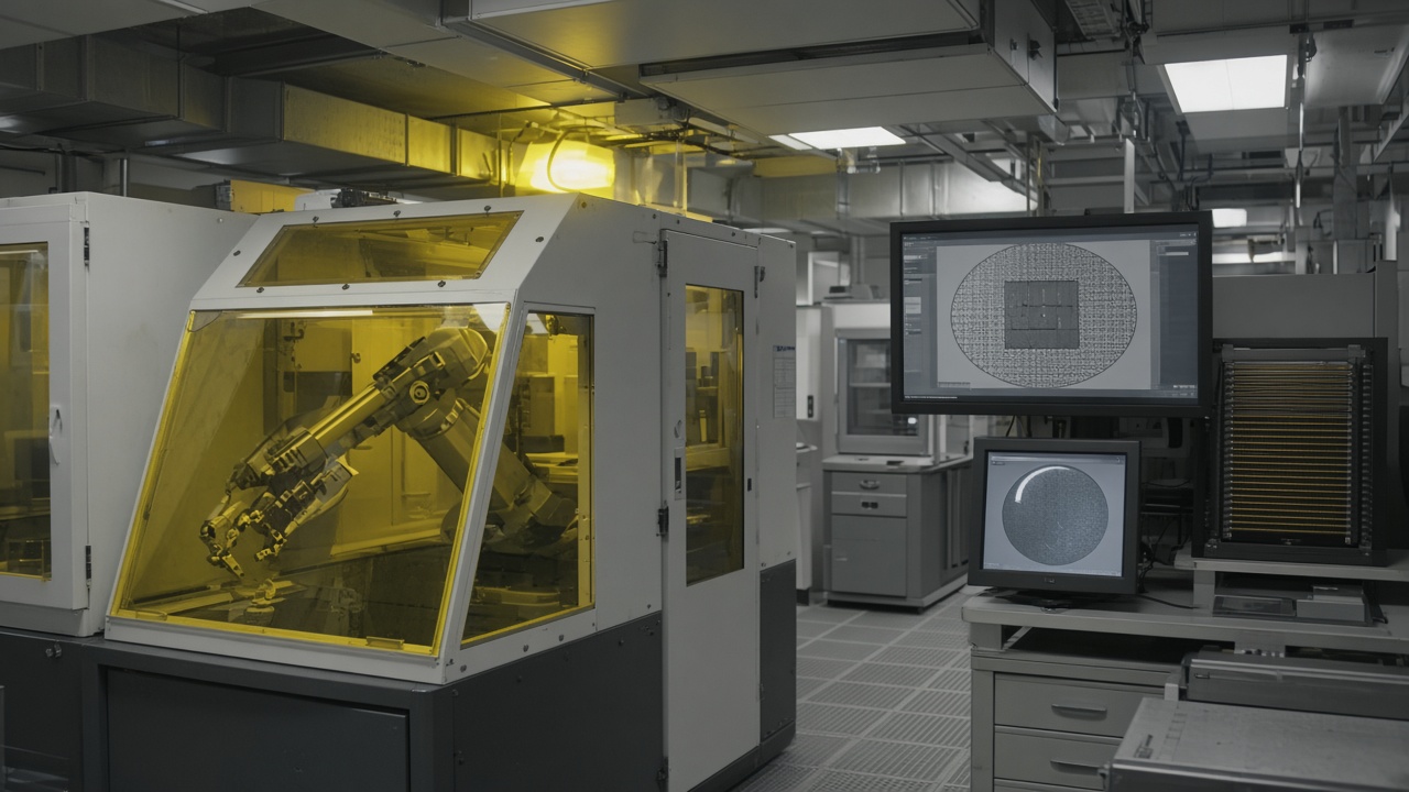
Rapidus Corp and IBM expanded an on-site AI inspection pact for the Hokkaido pilot fabrication line, rolling vision models that flag wafer defects before clean-room engineers sign off lots tied to Japan’s bid for advanced logic production. Mei Kobayashi’s AI desk reads the deal as operational glue—not a new chip architecture—meant to shrink yield learning curves while Rapidus races toward a late-decade mass-production target backed by METI subsidies and IBM process know-how.
What the models do
High-resolution cameras on lithography and etch tools feed convolutional networks trained on Rapidus-specific defect libraries. The system scores anomalies, routes flagged wafers to human review, and logs features for retraining when engineers confirm false positives. IBM hosts the training pipeline; inference runs on edge servers inside the fab to keep lot data from leaving the air-gapped segment.
Early metrics cited in partner briefings show double-digit reductions in average review time per lot, with bigger gains on repetitive particle classes common in new lines.
Why inspection AI matters now
Greenfield fabs lack years of human pattern recognition. Japan’s semiconductor revival strategy bets that software can compress yield ramps that took incumbents a decade. Rapidus must prove it can mirror 2-nanometer-class flows imported from IBM before domestic customers trust volume commitments.
AI inspection also offsets staffing shortages in northern Japan, where housing and winter weather complicate technician recruitment. Automating first-pass screening lets senior engineers focus on root-cause fixes rather than microscope hours.
Governance and risk
METI’s AI guidelines for critical infrastructure emphasize traceability: Rapidus must retain audit trails when models override or miss defects that later fail electrical test. IBM’s enterprise AI governance toolkit supplies versioning; Rapidus owns liability if a bad lot ships.
Export-control rules on advanced AI accelerators still shape which GPUs sit in the training cluster. Partners declined to name chip vendors in materials reviewed for this article.
Competitive field
TSMC and Samsung already deploy similar vision stacks; Rapidus’s twist is pairing IBM’s node roadmap with Japan-specific supplier mixes. Domestic equipment makers hope inspection data will feed back into tool calibration contracts.
Investors should not treat inspection AI as revenue—it is capex efficiency. Equity catalysts remain customer logos, subsidy disbursements, and tape-out milestones.
What would change the narrative
A high-profile miss where AI cleared a fatal defect would force manual fallbacks and political scrutiny on METI oversight. Conversely, published yield curves approaching incumbent norms would strengthen Rapidus bond financing talks rumored for next year.
For now, the IBM pact is a factory-floor story: fewer microscope hours, faster feedback loops, and another checkbox on Japan’s chip comeback slide deck.
Workforce and housing
Rapidus dormitory capacity in Chitose expanded this quarter to house additional inspection technicians recruited from Tohoku fabs. Local governments offered tax incentives for child-care centers to keep dual-income families in Hokkaido—human infrastructure matters as much as GPU racks.
Union liaison groups asked for transparency when AI scores influence performance reviews; management pledged human sign-off on any disciplinary use of model outputs.
Supplier ecosystem
Domestic lens and lighting vendors near Rapidus’s campus are bidding to supply camera modules tuned for yellow safelight environments. METI’s supplier database lists twelve tier-two firms cleared for on-site installation work this winter.
Timeline to production
Rapidus still targets mass production before 2030; inspection AI shaves weeks off yield learning but does not replace EUV tool delivery schedules. IBM executives visiting Hokkaido this month signed off on phase-two model training using synthetic defect injections—a standard step before live lot data dominates the corpus.