Rapidus Corporation is integrating Cadence Design Systems’ InnoStack AI Super Agent into its Raads agentic design environment, aiming to cut advanced SoC turnaround time while Chitose’s IIM-1 campus races toward mass production of 2-nanometer gate-all-around logic in the second half of fiscal 2027. The July partnership is a bet that software velocity can partially offset the commercial gap Rapidus still faces: dozens of active customer talks, but no public binding volume deals yet against TSMC and Samsung lines already shipping 2nm-class silicon.
What the Cadence tie-up actually does
Press releases from Rapidus and Cadence describe InnoStack orchestrating tasks across architecture, implementation, and signoff when paired with Raads Navigator and Indicator modules—marketing names for a workflow Japan’s state-backed foundry hopes will feel native to fabless startups intimidated by leading-edge PDK complexity. Rapidus publicly targets up to a twofold improvement in design turnaround versus traditional flows, a ratio that remains a goal until customers publish tape-out dates.
CEO Atsuyoshi Koike’s quoted pitch ties the integration to an “AI-native foundry” where agents sit beside EUV tools in Chitose, not just inside EDA licenses sold from San Jose. That narrative matters politically: METI’s subsidy story needs proof that Japanese fabs differ on more than geography.
Chitose milestones on the ground
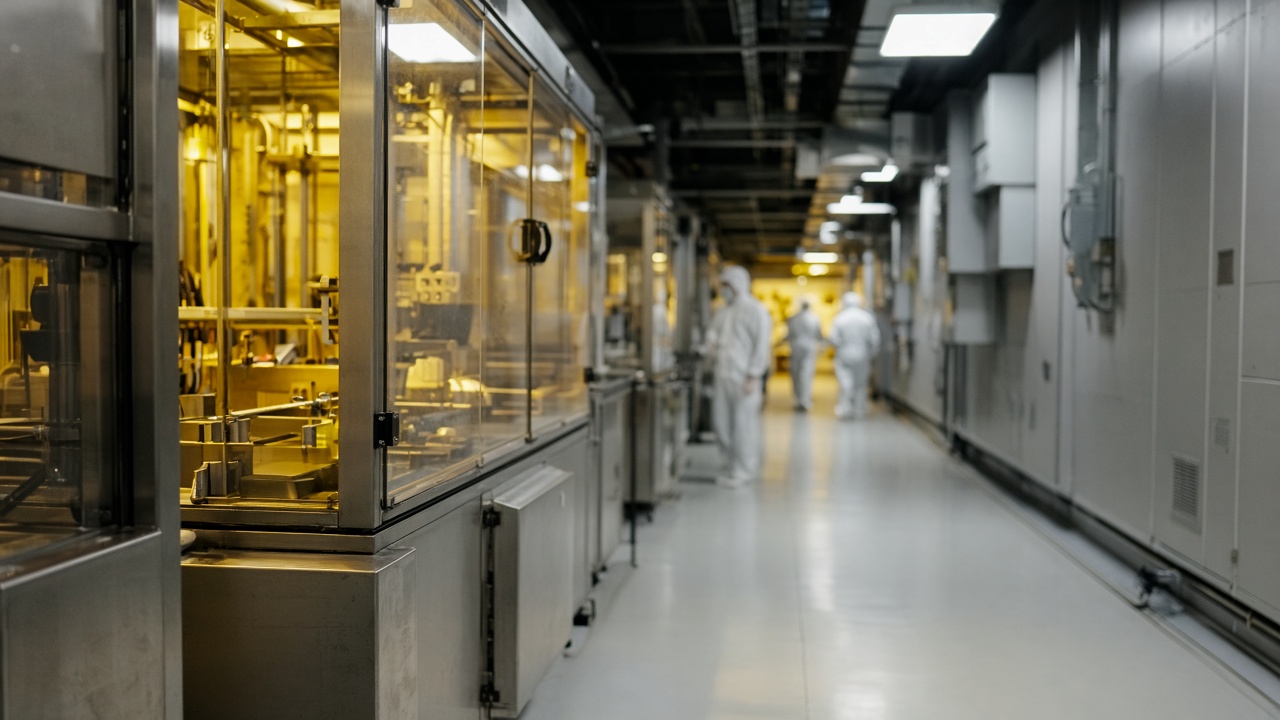
Rapidus’s IIM site documents a pilot line opening in April 2025, installation of Japan’s first mass-production-class ASML EUV tool in December 2024, and a mass-production target in 2027 at the Bibi World industrial park in Chitose, Hokkaido. Tom’s Hardware summarized a business plan filed with METI calling for roughly six thousand wafer starts per month at launch, scaling toward twenty-five thousand within a year—ambitious for a first-time leading-edge entrant and sensitive to yield curves Rapidus has not disclosed publicly.
What investors can verify: concrete poured, tools delivered, PDK drops to early adopters in early 2026 after a July 2025 demonstration of working 2nm GAA transistors. What they cannot: yield percentages or named anchor customers— the commercial cliff Jordan Ellis tracks when asking whether the next round exists if wafers do not ship on spec.
Round, rescue, or strategic valuation
February 2026 financing reportedly topped ¥267 billion with government and corporate backers including Sony and SoftBank, signaling rescue-scale capital rather than a typical Series B. Equity stories here are national industrial policy: dilution is spread across strategic investors who also might buy wafers. The Cadence deal is not a cash round; it is capability packaging to make Raads sticky before customers commit volume.
Without signed take-or-pay agreements, Rapidus remains a pilot glorified by press releases—a harsh framing Koike’s team disputes by citing more than sixty active negotiations. Until one logo appears on a volume contract, external analysts will treat InnoStack integration as engineering optionality, not revenue.
Competitive clock
TSMC and Samsung already market 2nm timelines to Apple-class giants; Rapidus pitches smaller lot sizes, shorter cycle times, and AI-assisted design for automotive and edge AI chips that cannot secure Taiwan priority. Intel’s 18A campaign competes for the same skeptical fabless accounts. Rapidus must show that Raads plus InnoStack shrinks months off taping out, not merely slides off PowerPoints at CadenceLIVE Japan keynotes.
Hokkaido location adds logistics costs but promises earthquake diversity from Kumamoto-era trauma—a selling point to Japanese system houses even if global players yawn.
What could break the plan
Yield stalls would push mass output into 2028 despite METI slides, triggering another capital call. Design-agent hype could outrun reliability if automated flows miss corner cases on first silicon. Export-control shifts on EUV spare parts or EDA features would hurt Raads integrations tied to U.S. vendors—Cadence included.
Jordan Ellis’s one-sentence business test: Rapidus is a government-backed 2nm bet that design agents must convert pilot PDK success into paid wafer starts before Chitose depreciation overwhelms the balance sheet.
Next checkpoints
Watch for customer co-announcements at industry conferences this autumn, PDK revision notes citing InnoStack hooks, and METI progress reports on wafer-start ramps. A twofold TAT claim needs a named SoC and a date; without that, the Cadence deal is scaffolding for 2027 mass output still defined more by concrete in Chitose than by agents on a slide.